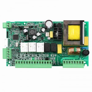
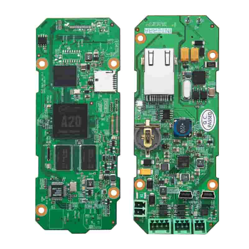
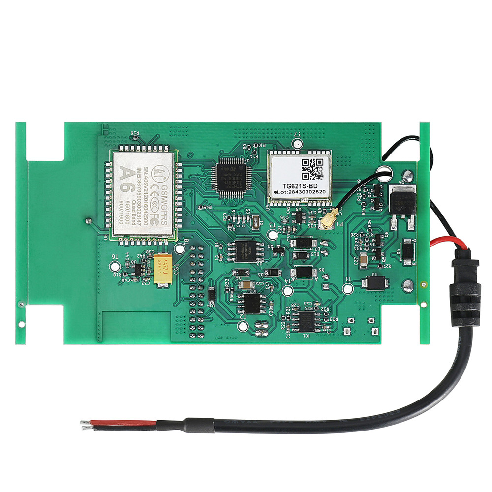
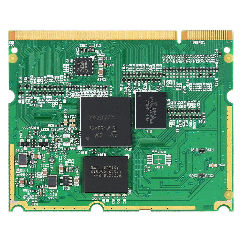
Vehicle Electronics PCBA board
Products feature
● -Reliability testing
● -Traceability
● -Thermal management
● -Heavy copper ≥ 105um
● -HDI
● -Semi - flex
● -Rigid - flex
● -High frequency milimeter microwave
PCB structure characteristics
1. Dielectric layer (Dielectric): It is used to maintain the insulation between lines and layers, commonly known as the substrate.
2. Silkscreen (Legend/Marking/Silkscreen): This is a non-essential component. Its main function is to mark the name and position box of each part on the circuit board, which is convenient for maintenance and identification after assembly.
3.Surface treatment (SurtaceFinish): Since the copper surface is easily oxidized in the general environment, it cannot be tinned (poor solderability), so the copper surface to be tinned will be protected. The protection methods include HASL, ENIG, Immersion Silver, Immersion TIn, and organic solder preservative (OSP). Each method has its own advantages and disadvantages, collectively referred to as surface treatment.
PCB Techinecal Capacity
| Layers | Mass production: 2~58 layers / Pilot run: 64 layers |
| Max. Thickness | Mass production: 394mil (10mm) / Pilot run: 17.5mm |
| Material | FR-4 (Standard FR4, Mid-Tg FR4,Hi-Tg FR4, Lead free assembly material) , Halogen-Free, Ceramic filled , Teflon, Polyimide, BT, PPO, PPE, Hybrid, Partial hybrid, etc. |
| Min. Width/Spacing | Inner layer: 3mil/3mil (HOZ), Outer layer: 4mil/4mil(1OZ) |
| Max. Copper Thickness | UL certificated: 6.0 OZ / Pilot run: 12OZ |
| Min. Hole Size | Mechanical drill: 8mil(0.2mm) Laser drill: 3mil(0.075mm) |
| Max. Panel Size | 1150mm × 560mm |
| Aspect Ratio | 18:1 |
| Surface Finish | HASL,Immersion Gold, Immersion Tin, OSP, ENIG + OSP, Immersion Silver, ENEPIG, Gold Finger |
| Special Process | Buried Hole, Blind Hole, Embedded Resistance, Embedded Capacity, Hybrid, Partial hybrid, Partial high density, Back drilling, and Resistance control |