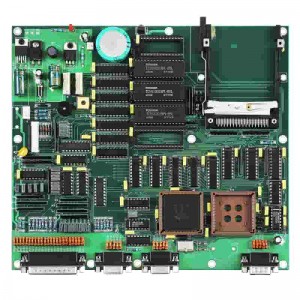
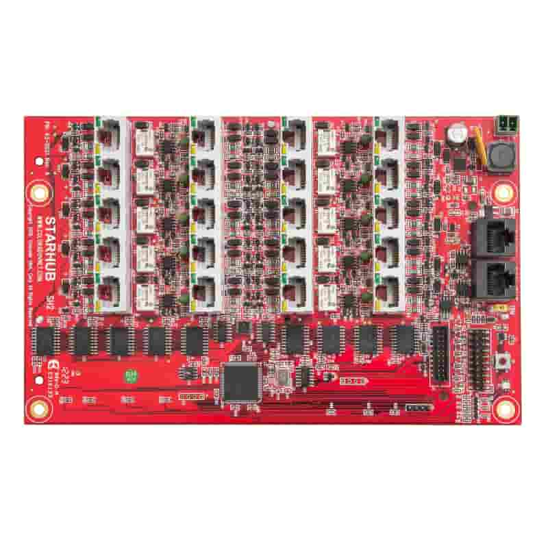
One stop electronic Server PCBA board manufacturer
Products feature
● Material: Fr-4
● Layer Count: 6 layers
● PCB Thickness: 1.2mm
● Min. Trace / Space Outer: 0.102mm/0.1mm
● Min. Drilled Hole: 0.1mm
● Via Process: Tenting Vias
● Surface Finish: ENIG
PCB structure characteristics
1. Circuit and pattern (Pattern): The circuit is used as a tool for conducting between components. In the design, a large copper surface will be designed as a grounding and power supply layer. Lines and drawings are made at the same time.
2. Hole (Throughole/via): The through hole can make the lines of more than two levels conduct each other, the larger through hole is used as a component plug-in, and the non-conductive hole (nPTH) is usually used as the surface Mounting and positioning, used for fixing screws during assembly.
3. Solderresistant ink (Solderresistant/SolderMask): Not all copper surfaces have to eat tin parts, so the non-tin-eaten area will be printed with a layer of material (usually epoxy resin) that isolates the copper surface from eating tin to avoid non-soldering. There is a short circuit between the tinned lines. According to different processes, it is divided into green oil, red oil and blue oil.
4. Dielectric layer (Dielectric): It is used to maintain the insulation between lines and layers, commonly known as the substrate.
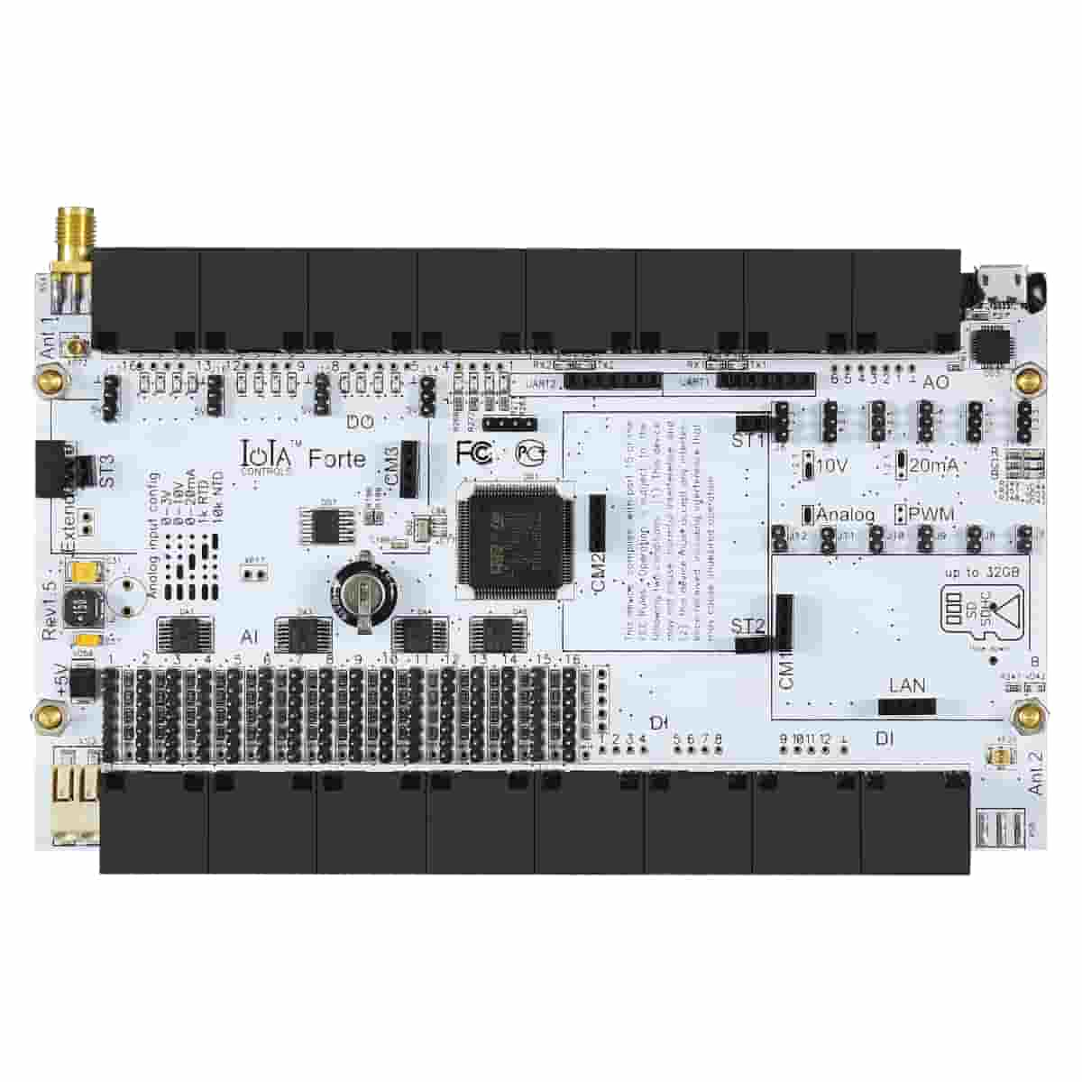
PCBA technical Capacity
| SMT | Position accuracy:20 um |
| Components size:0.4×0.2mm(01005) —130×79mm,Flip-CHIP,QFP,BGA,POP | |
| Max. component height::25mm | |
| Max. PCB size:680×500mm | |
| Min. PCB size:no limited | |
| PCB thickness:0.3 to 6mm | |
| PCB weight:3KG | |
| Wave-Solder | Max. PCB width:450mm |
| Min. PCB width: no limited | |
| Component height:Top 120mm/Bot 15mm | |
| Sweat-Solder | Metal type :part, whole, inlay, sidestep |
| Metal material:Copper , Aluminum | |
| Surface Finish:plating Au, plating sliver , plating Sn | |
| Air bladder rate:less than 20% | |
| Press-fit | Press range:0-50KN |
| Max. PCB size:800X600mm | |
| Testing | ICT,Probe flying,burn-in,function test,temperature cycling |