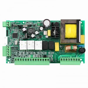
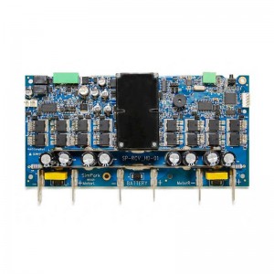
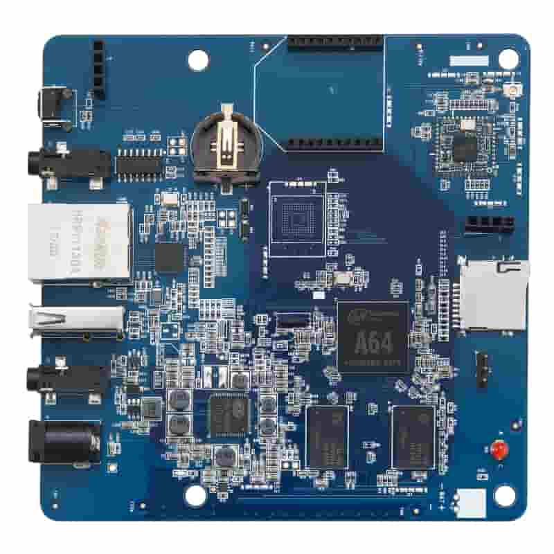
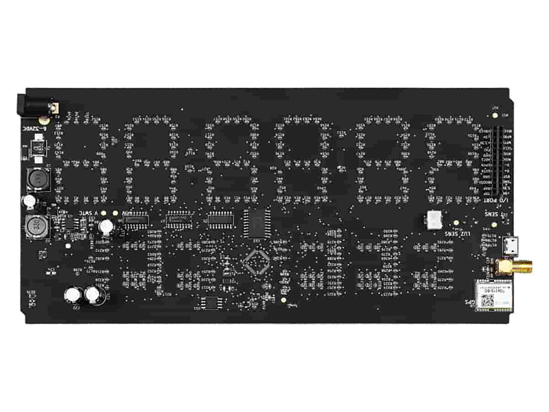
Medical Electronics PCBA board manufacturer
CAPABILITIES
● -Layer Count: 2L/4L/6L/8L/10L
● -Max. Delivery Panel Size: 699mm×594mm
● -Max. Copper Weight (Inner/Outer Layer): 12oz
● -Max.Board Thickness: 5.0mm
● -Max. Aspect Ratio: 15:1
● -Surface Finish: LF-HASL, ENIG, Imm-Ag, Imm-Sn, OSP, ENEPIG, Gold Finger
PCB structure characteristics
1. Circuit and pattern (Pattern): The circuit is used as a tool for conducting between components. In the design, a large copper surface will be designed as a grounding and power supply layer. Lines and drawings are made at the same time.
2.Hole (Throughole/via): The through hole can make the lines of more than two levels conduct each other, the larger through hole is used as a component plug-in, and the non-conductive hole (nPTH) is usually used as the surface Mounting and positioning, used for fixing screws during assembly.
3.Silkscreen (Legend/Marking/Silkscreen): This is a non-essential component. Its main function is to mark the name and position box of each part on the circuit board, which is convenient for maintenance and identification after assembly.
PCBA technical Capacity
| SMT | Position accuracy:20 um |
| Components size:0.4×0.2mm(01005) —130×79mm,Flip-CHIP,QFP,BGA,POP | |
| Max. component height::25mm | |
| Max. PCB size:680×500mm | |
| Min. PCB size:no limited | |
| PCB thickness:0.3 to 6mm | |
| PCB weight:3KG | |
| Wave-Solder | Max. PCB width:450mm |
| Min. PCB width: no limited | |
| Component height:Top 120mm/Bot 15mm | |
| Sweat-Solder | Metal type :part, whole, inlay, sidestep |
| Metal material:Copper , Aluminum | |
| Surface Finish:plating Au, plating sliver , plating Sn | |
| Air bladder rate:less than 20% | |
| Press-fit | Press range:0-50KN |
| Max. PCB size:800X600mm | |
| Testing | ICT,Probe flying,burn-in,function test,temperature cycling |
The medical industry has revolutionized the way we approach health and wellness. With the advancement of science and technology, people's living standards and health awareness have improved significantly. As a result, the demand for medical equipment and instruments has skyrocketed.
Medical electronics have played a vital role in this transition. They have proven indispensable in diagnosing disease, monitoring vital signs, and even administering treatment. One of the key components of these medical electronics is the printed circuit board assembly (PCBA) board.
Our medical electronic PCBA boards are specially designed to meet the high standards and stringent requirements of the medical industry. With its outstanding reliability and performance, it has become the first choice of medical equipment manufacturers around the world.
Our PCBA boards are available in a variety of layer counts including 2L, 4L, 6L, 8L and 10L, allowing flexibility and customization to the specific needs of the medical device that will be integrated. This versatility ensures that our PCBA boards can accommodate even the most complex medical electronics.
In addition, the maximum delivered panel size of our PCBA board is 699mm×594mm, which provides ample space for the integration of various components and functions. This enables greater functionality and improves the overall performance of medical devices.
Additionally, the inner and outer layers of our PCBA boards can handle up to 12 ounces of copper, ensuring optimum conductivity and stability. This feature is critical in medical electronics as it helps prevent any signal interference or interruption, which could adversely affect the accuracy and efficacy of the device.
We know that the thickness of PCBA board is a crucial factor for medical electronic products. Therefore, our boards can accommodate a maximum thickness of 5.0mm, meeting various mounting and housing requirements for different devices.
Additionally, our PCBA boards have a maximum aspect ratio of 15:1, enabling the integration of complex and compact designs. This is especially beneficial for medical electronics, where space is often limited and each component needs to be placed strategically for optimal function.
To ensure the durability and longevity of our PCBA boards, we offer a range of surface treatments. These include LF-HASL, ENIG, Imm-Ag, Imm-Sn, OSP, ENEPIG, and Gold Finger. Each finish has been carefully selected to provide superior protection against abrasion, moisture and other environmental elements, ensuring PCB reliability.
All in all, our medical electronics PCBA boards are game changers in the medical industry. With its outstanding features including various layer counts, maximum delivered panel sizes, copper weights, board thicknesses, aspect ratios and surface finish options, it guarantees unmatched performance and reliability. By choosing our PCBA boards, medical device manufacturers can confidently develop cutting-edge healthcare solutions that improve patient outcomes and revolutionize the healthcare landscape.
FAQ
Basically NO MOQ For Most Prooducts, Trail Oeder Or Sample Order Will Be Acceptable.
Most Of Our Products Are With 6 Months Quality Warranty.
Customized Logo For Products Or Package Will Be Highly Welcomed.We Made A lot For Our Customers.
Pls Confirm With Us The Modle You Need.And The Sample Fee Will Be Refunded In Bulk.
Sample Will Be Send Out Within 2days After Received Payment.
Normally It Takes 5 Working Days After Received Payment.
100% QC Before Shipment. If There're Some Unexpected Problem Happan, Like Quality Problem