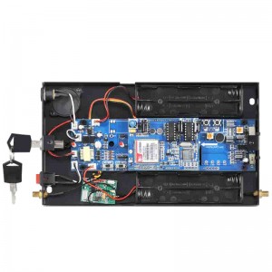
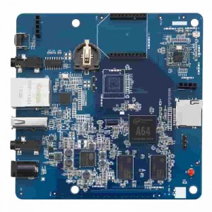
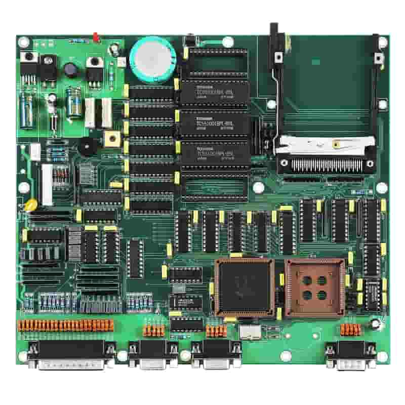
Computer and Peripherals PCBA board
Products feature
● -Material: Fr-4
● -Layer Count: 14 layers
● -PCB Thickness: 1.6mm
● -Min. Trace / Space Outer: 4/4mil
● -Min. Drilled Hole: 0.25mm
● -Via Process: Tenting Vias
● -Surface Finish: ENIG
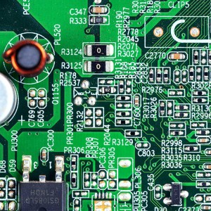
PCB structure characteristics
1. Solderresistant ink (Solderresistant/SolderMask): Not all copper surfaces have to eat tin parts, so the non-tin-eaten area will be printed with a layer of material (usually epoxy resin) that isolates the copper surface from eating tin to avoid non-soldering. There is a short circuit between the tinned lines. According to different processes, it is divided into green oil, red oil and blue oil.
2. Dielectric layer (Dielectric): It is used to maintain the insulation between lines and layers, commonly known as the substrate.
3. Surface treatment (SurtaceFinish): Since the copper surface is easily oxidized in the general environment, it cannot be tinned (poor solderability), so the copper surface to be tinned will be protected. The protection methods include HASL, ENIG, Immersion Silver, Immersion TIn, and organic solder preservative (OSP). Each method has its own advantages and disadvantages, collectively referred to as surface treatment.
PCB Techinecal Capacity
| Layers | Mass production: 2~58 layers / Pilot run: 64 layers |
| Max. Thickness | Mass production: 394mil (10mm) / Pilot run: 17.5mm |
| Material | FR-4 (Standard FR4, Mid-Tg FR4,Hi-Tg FR4, Lead free assembly material) , Halogen-Free, Ceramic filled , Teflon, Polyimide, BT, PPO, PPE, Hybrid, Partial hybrid, etc. |
| Min. Width/Spacing | Inner layer: 3mil/3mil (HOZ), Outer layer: 4mil/4mil(1OZ) |
| Max. Copper Thickness | UL certificated: 6.0 OZ / Pilot run: 12OZ |
| Min. Hole Size | Mechanical drill: 8mil(0.2mm) Laser drill: 3mil(0.075mm) |
| Max. Panel Size | 1150mm × 560mm |
| Aspect Ratio | 18:1 |
| Surface Finish | HASL,Immersion Gold, Immersion Tin, OSP, ENIG + OSP, Immersion Silver, ENEPIG, Gold Finger |
| Special Process | Buried Hole, Blind Hole, Embedded Resistance, Embedded Capacity, Hybrid, Partial hybrid, Partial high density, Back drilling, and Resistance control |