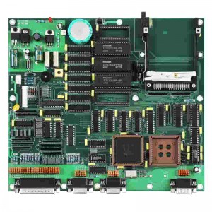
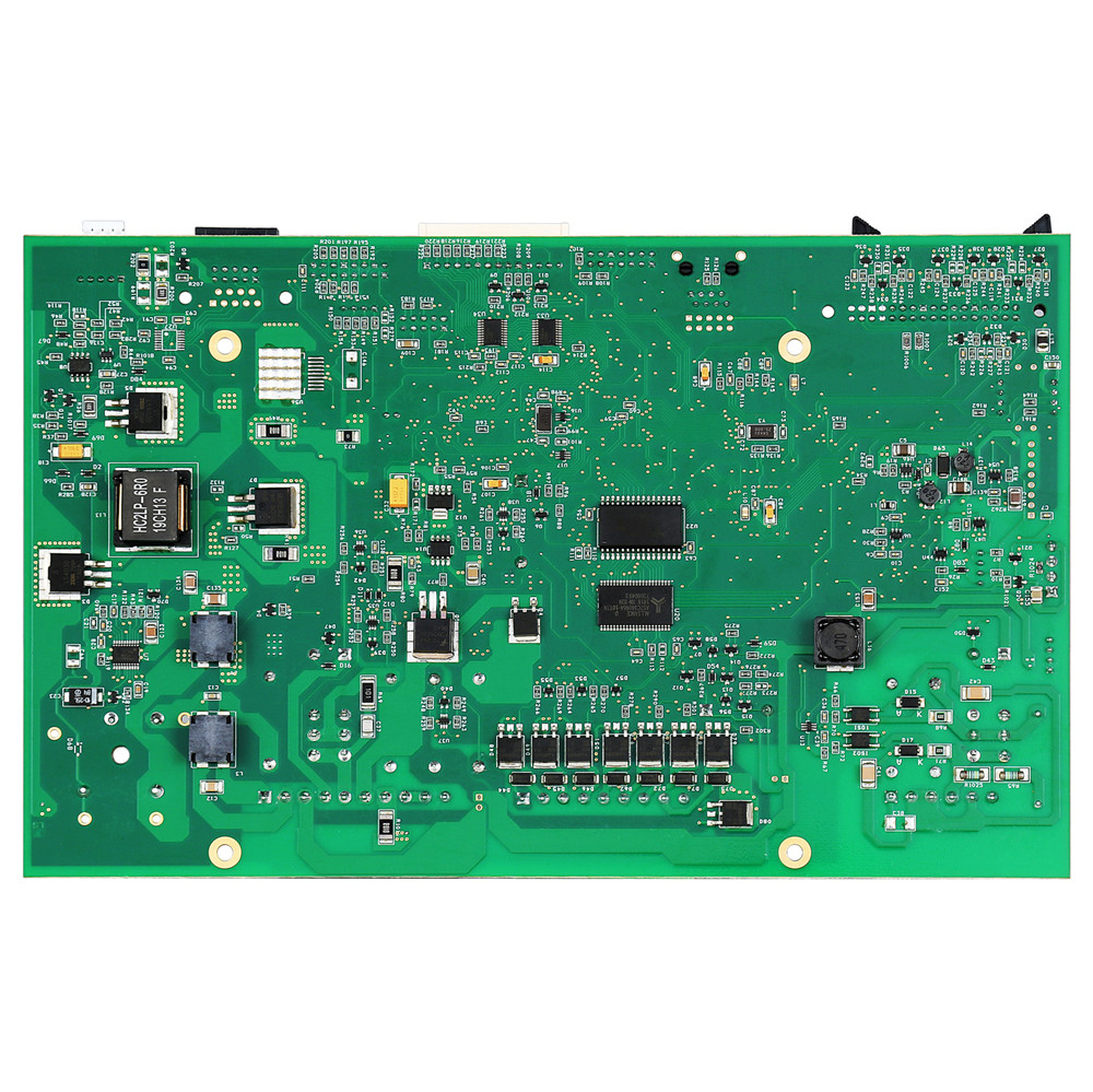
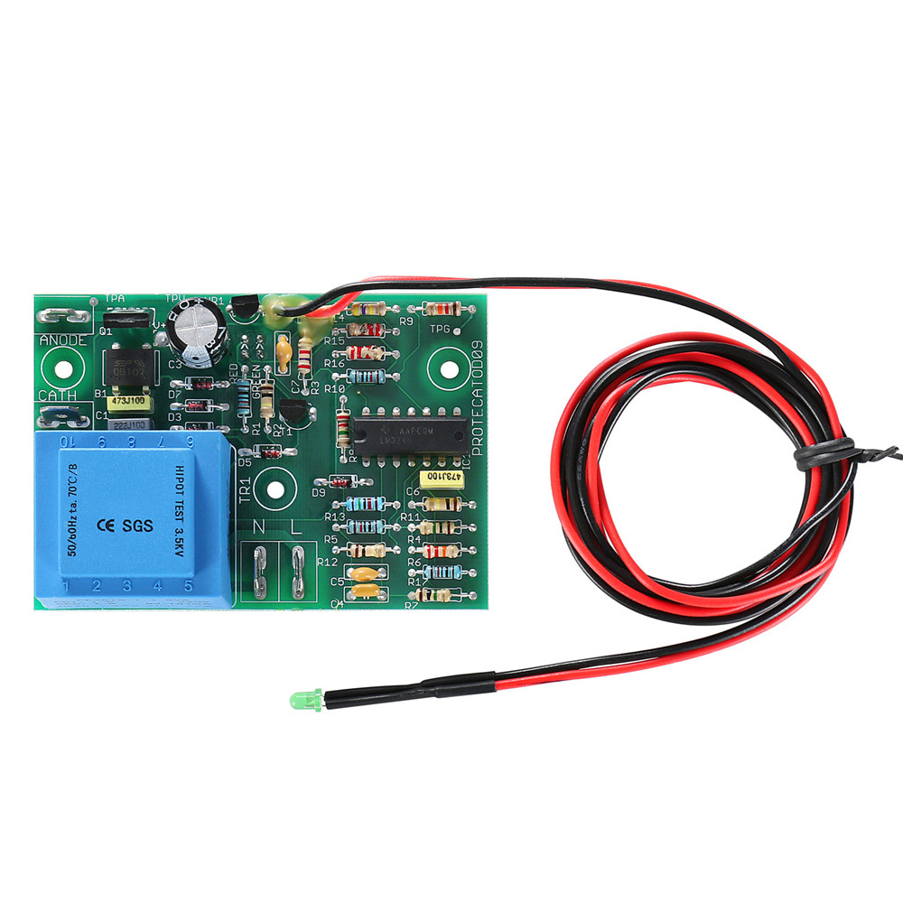
One stop electronic safety PCBA board

Products feature
● Material: Fr-4
● Layer Count: 6 layers
● PCB Thickness: 1.2mm
● Min. Trace / Space Outer: 0.102mm/0.1mm
● Min. Drilled Hole: 0.1mm
● Via Process: Tenting Vias
● Surface Finish: ENIG
Advantage
1) Years of experience in half-hole production, using Da Chuan Routing machine, routing the half- hole then routing the shape, meet the strict shape requirements;
2) Minimum line width and line spacing: 0.065/0.065mm, minimum BGA pad: 0.2mm, meet customer's special needs;
3) Electroplated Copper Flling of Blind Holes by Universal DVCP(Double Track Vertical Continuous Copper Plating Equip ment) to ensure that there are no voids in the holes and quality of customer products;
4) Strict sampling inspection mode, guarantee customers' product yield.
PCBA technical Capacity
| SMT | Position accuracy:20 um |
| Components size:0.4×0.2mm(01005) —130×79mm,Flip-CHIP,QFP,BGA,POP | |
| Max. component height::25mm | |
| Max. PCB size:680×500mm | |
| Min. PCB size:no limited | |
| PCB thickness:0.3 to 6mm | |
| PCB weight:3KG | |
| Wave-Solder | Max. PCB width:450mm |
| Min. PCB width: no limited | |
| Component height:Top 120mm/Bot 15mm | |
| Sweat-Solder | Metal type :part, whole, inlay, sidestep |
| Metal material:Copper , Aluminum | |
| Surface Finish:plating Au, plating sliver , plating Sn | |
| Air bladder rate:less than 20% | |
| Press-fit | Press range:0-50KN |
| Max. PCB size:800X600mm | |
| Testing | ICT,Probe flying,burn-in,function test,temperature cycling |
Our innovative approach allows us to combine the antenna and signal processing into a single package, eliminating integration challenges. Not only does this save you time and effort, it also ensures shorter signal paths, reducing signal loss during transmission and processing.
Carefully crafted from high-quality materials, our PCBA boards are made of Fr-4, a reliable and durable material known for its excellent electrical properties and mechanical strength. The board has 6 layers, providing ample space for all necessary components while maintaining optimal functionality.
Our PCBA boards are 1.2 mm thick, ensuring the highest precision and seamless integration into your security system. 0.102mm/0.1mm minimum trace external and spatial measurements provide high accuracy for superior performance in safety systems.
Drilled holes with a minimum diameter of 0.1 mm further enhance the functionality of the PCB and compatibility with various security devices. We use a tented via process to protect the drilled holes from damage and ensure reliable connections between the different layers of the board.
In order to ensure the service life and reliability of the PCBA board, we use electroless nickel immersion gold (ENIG) for surface treatment. This surface treatment provides excellent chemical and electrical performance, prevents corrosion and ensures optimal signal transmission.
Trust our expertise and experience in the electronics manufacturing industry. We are committed to providing high-quality products that meet the stringent requirements of the security industry. Invest in our one-stop electronic safety PCBA boards and experience seamless integration, compact design and superior performance.