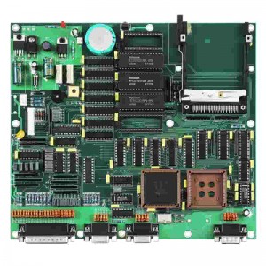
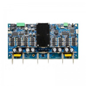
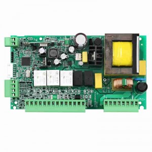
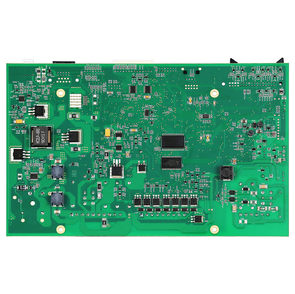
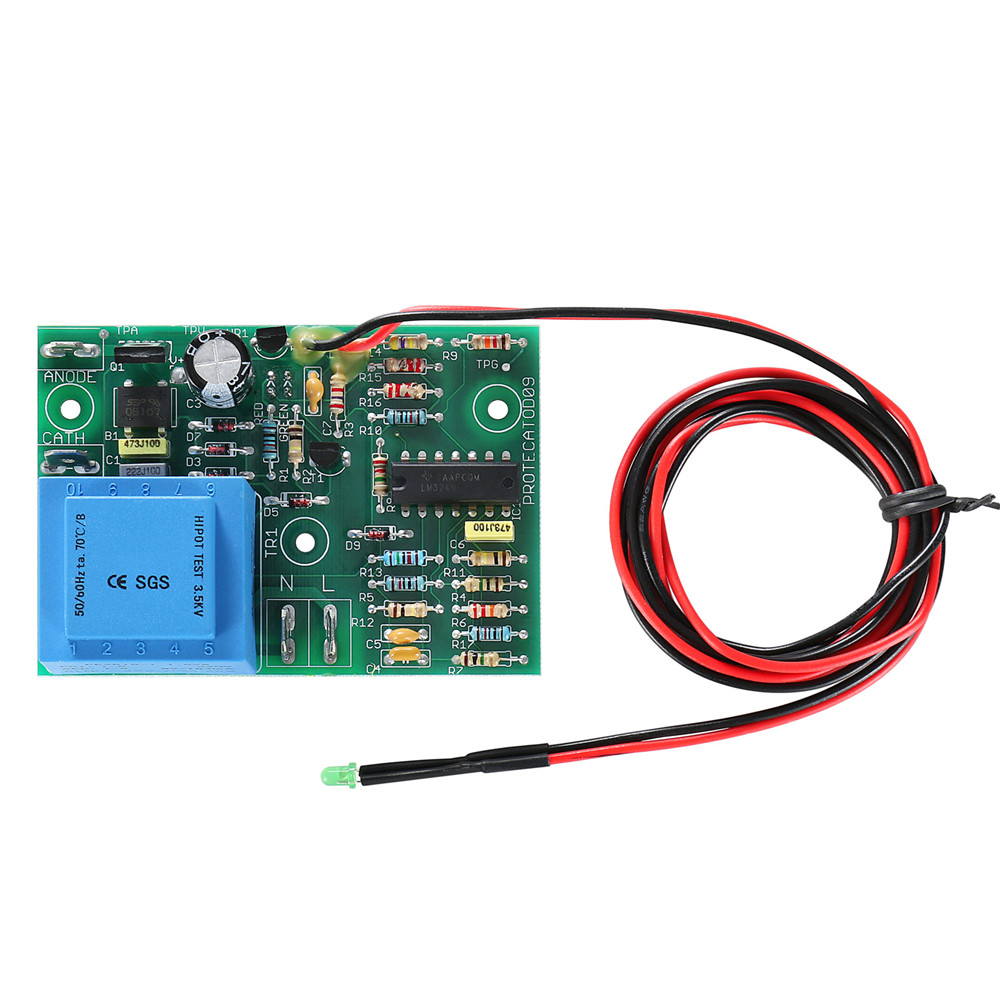
One stop electronic Security PCBA board manufacturer

Products feature
● Material: Fr-4
● Layer Count: 6 layers
● PCB Thickness: 1.2mm
● Min. Trace / Space Outer: 0.102mm/0.1mm
● Min. Drilled Hole: 0.1mm
● Via Process: Tenting Vias
● Surface Finish: ENIG
Advantage
1) Years of experience in half-hole production, using Da Chuan Routing machine, routing the half- hole then routing the shape, meet the strict shape requirements;
2) Minimum line width and line spacing: 0.065/0.065mm, minimum BGA pad: 0.2mm, meet customer's special needs;
3) Electroplated Copper Flling of Blind Holes by Universal DVCP(Double Track Vertical Continuous Copper Plating Equip ment) to ensure that there are no voids in the holes and quality of customer products;
4) Strict sampling inspection mode, guarantee customers' product yield.
PCBA technical Capacity
| SMT | Position accuracy:20 um |
| Components size:0.4×0.2mm(01005) —130×79mm,Flip-CHIP,QFP,BGA,POP | |
| Max. component height::25mm | |
| Max. PCB size:680×500mm | |
| Min. PCB size:no limited | |
| PCB thickness:0.3 to 6mm | |
| PCB weight:3KG | |
| Wave-Solder | Max. PCB width:450mm |
| Min. PCB width: no limited | |
| Component height:Top 120mm/Bot 15mm | |
| Sweat-Solder | Metal type :part, whole, inlay, sidestep |
| Metal material:Copper , Aluminum | |
| Surface Finish:plating Au, plating sliver , plating Sn | |
| Air bladder rate:less than 20% | |
| Press-fit | Press range:0-50KN |
| Max. PCB size:800X600mm | |
| Testing | ICT,Probe flying,burn-in,function test,temperature cycling |
Write your message here and send it to us